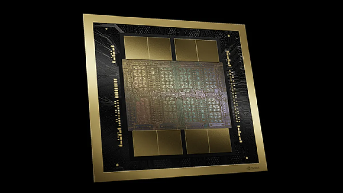
There is a new Nvidia structure on the town, and it is a doozy. Blackwell has simply been introduced by Nvidia’s CEO Jensen Huang at GTC and can function contained in the ludicrously giant B200 GPU. To name them ‘GPUs’ would technically be flawed, nevertheless. They’re dual-GPU packages with a complete of 208 billion transistors throughout them. To place that into perspective, the earlier must-have compute chips out of Nvidia, the Hopper H200 and H100, has simply over 80 billion transistors. An RTX 4090 has 76.3 million. We’re taking a look at over double that with Blackwell, which makes a whole lot of sense contemplating it is dual-wielding GPUs and a brand new chip-to-chip interconnect.
Blackwell is sadly not for gaming. Boo! I am unsure our financial institution accounts can be prepared for such a mighty factor anyhow. Blackwell is usually supposed for rollout inside knowledge centres chasing larger and larger compute figures. Why? Synthetic intelligence, largely.
However since we’re awaiting any information on the next-generation GeForce graphics playing cards, let’s take into accout which options would possibly find yourself being transplanted from these mahoosive Blackwell chips into no matter structure turns up within the subsequent graphics playing cards for gaming—which is also Nvidia Blackwell, albeit a stripped-down model, as we cannot want the entire gubbins included with the B200/B100.
Let’s begin with one thing we most likely will see in a GeForce GPU in future: Blackwell options new fifth-generation Tensor Cores. These are accelerators for directions largely used inside AI functions, i.e. inference and coaching, and the fifth-gen variations are set to bump efficiency by as much as 30 instances. The brand new Tensor Cores embrace precision codecs and an up to date Transformer Engine, which was first launched with Hopper, to speed up inference and coaching of huge language fashions.
Since GeForce playing cards use Tensor Cores for options similar to DLSS, and we have already seen fourth-generation Tensor Cores make the leap from Nvidia’s enterprise-only Hopper structure into the Ada Lovelace structure powering the RTX 40-series, we’re more likely to see the identical occur with the next-gen. Although how these extra options shall be leveraged by Nvidia would be the key factor: a brand new DLSS model or Body Era function can be the doubtless candidates for additional growth.
Beneath: flick via the gallery for a step-by-step of how every a part of the Blackwell bundle comes collectively.
Picture 1 of 3

The Blackwell B200 and B100 each seem minimize from the identical material. The B200 gives greater compute efficiency throughout the bigger HGX B200 system (made up of eight B200 GPUs) than the B100 does within the HGX B100 system (made up of eight B100 GPUs) at 40TFLOPs FP64 to 30 TFLOPs FP64, however efficiency seems shut sufficient for us to presume each B200 and B100 constructed out of the identical mammoth 208 billion transistor bundle.
“It is okay, Hopper,” says Huang as he holds the gargantuan Blackwell bundle subsequent to a Hopper die.
| Row 0 – Cell 0 | B200 |
| Structure | Blackwell |
| Transistors | 208 billion (2x 10⁴B) |
| Course of node | TSMC 4NP |
| Tensor Cores | fifth Gen |
| No. of Tensor Cores | ? |
| No. of CUDA Cores | ? |
| Clock pace | ? |
| Reminiscence | HBM3e |
| Reminiscence capability | 192 GB |
| Worth | lol |
The Blackwell chip options two GPUs seen to be performing as a single chip—every GPU constructed at what’s often called the reticle restrict, which is basically the utmost manufacturable dimension for a single chip in any given lithographic course of. As Huang notes throughout his keynote: “There is a small line between two dies, that is the primary time two dies have abutted like this collectively in such a means that the 2 dies suppose it is one chip.”
Nvidia has performed round with splitting GPUs earlier than. The Ampere GA100 GPU was kind of break up down the center into two halves with an interconnect, although the precise silicon wasn’t. Blackwell makes that additional leap with two correctly sliced silicon halves.
4 years in the past, we break up GA100 into two halves that talk via an interconnect. It was a giant transfer – and but barely anybody seen, because of superb work from CUDA and the GPU group.In the present day, that work involves fruition with the Blackwell launch. Two dies. One superior GPU. https://t.co/XuaUQPskkM pic.twitter.com/svRKhwPYEnMarch 18, 2024
Will the identical dual-GPU design make it right into a gaming graphics card? It is fairly darn unlikely however not altogether not possible.
For starters, leaks counsel the largest graphics card within the next-generation Nvidia lineup, presumably the RTX 5090, will include many extra CUDA Cores than its predecessor, the RTX 4090. Although present rumours do not counsel any type of direct doubling of the RTX 4090 spec. Even when the RTX 5090 had been utilizing two smaller GPUs to make for a extra environment friendly chip, there are extra concrete explanation why a dual-GPU strategy might be unrealistically tough.
Getting two GPUs to run as one whereas gaming is enormously robust—that is why CrossFire and SLI are useless. For this multi-GPU strategy to work the 2 GPUs would wish to behave as one whereas necessitating subsequent to no modifications to the APIs that talk with a graphics card.
Huang does observe that “these two sides of the Blackwell chip don’t know which facet they’re on,” in reference to how the Blackwell GPU bundle works collectively as one. “There is no reminiscence locality points, no cache points. It is only one large chip,” Huang continues.
That does fill me with some hope of reaching a degree the place multi-GPU gaming dies are a risk, however that is nonetheless a tricky cookie to crack. It is simpler to do with compute chips, such because the B200, offered there’s loads of bandwidth between the 2 dies—therefore why there is a 10TB/s interconnect on the Blackwell GPU.
For now I feel it extra doubtless an up-to-date course of node would be the main means Nvidia goes about cramming extra cores right into a gaming chip. And that is one space the place Blackwell gives some indication of what to anticipate.
Picture 1 of 2
Above: Nvidia has prototype boards for some severely highly effective (and costly) programs utilizing Blackwell.
What we would see make the leap from Blackwell right into a next-gen gaming card is the usage of TSMC’s 4NP course of node. That is reportedly an extension of the customized 4N course of node created for and used solely by Nvidia’s Ada Blackwell and Hopper chips. It is probably not a 4nm course of node, nevertheless, being extra carefully associated to TSMC’s 5nm node. It is complicated however that is seemingly by design as virtually each main semiconductor producer does the identical factor. For instance, Intel 7 is definitely its 10nm course of, and what makes a course of 10nm anyhow? We might be right here some time. Level is, it is very doubtless we’ll see the next-gen GeForce playing cards utilizing the 4NP course of, too.
The Decompression Engine on Blackwell is one thing of specific curiosity to avid gamers. Nvidia launched RTX IO again in 2020 as a option to shift load from the CPU onto the GPU to hurry up recreation asset load instances. It is part of a wider trade push to combine GPU decompression into video games together with AMD’s SmartAccess Storage, Microsoft’s DirectStorage, and Khronos Group’s Vulkan API. All of them depend on an open GPU compression normal referred to as GDeflate.
Blackwell’s new Decompression Engine particularly accelerates GDeflate particularly, amongst different decompression requirements, and that might turn out to be useful for a wider push to undertake GDeflate in video games if it had been to even be built-in into next-gen GeForce GPUs. The quicker a GPU can decompress belongings, the quicker they are often loaded right into a recreation, and which means extra detailed recreation worlds might be designed with an affordable expectation of efficiency.
Now there are a number of elements of Blackwell unlikely to make it right into a future gaming GPU. The Reliability, Availability, and Serviceability (RAS) engine constructed to establish and report on faults or potential faults earlier than they happen. That is a function a lot handier if, like Meta, you are operating lots of of 1000’s of these items without delay. Equally, the concentrate on the TEE-I/O safety mannequin for “safe AI” will not be essentially on the agenda for GeForce. The flexibility to hook up heaps of GPUs collectively into one superchip or many superchips into one super-system utilizing NVLink may even get thrown on the sacrificial pyre of gaming.
Lastly, we cannot see lots of of gigabytes of HBM3e reminiscence on any RTX 50-series or comparable gaming chip. Nvidia’s Grace Blackwell Superchip, which contains two Blackwell GPUs and a Grace CPU, seems to be superior (and costly) with 384 GB of HBM3e reminiscence providing 16 TB/s bandwidth, however we’ll almost certainly be gaming on 8GB or extra (hopefully much more) of GDDR7 reminiscence.
A few potential graphics goodies from Blackwell which may make the leap right into a gaming graphics card, then, and some extra that most likely will not. Sadly we do not know after we would possibly discover out for sure. Nvidia hasn’t but given us a agency date for when next-gen gaming graphics playing cards will arrive. Nor when merchandise based mostly on Blackwell will arrive, for that matter. The corporate has little have to promote, nevertheless: Meta, Google, Microsoft, OpenAI, Oracle, xAI, Dell and Amazon are amongst its purchasers already lining up for a little bit of Blackwell.
If final era’s launch cadence is to be adopted, which had Hopper introduced in March and Ada Lovelace in September, then we could hear extra on next-gen GeForce graphics playing cards shortly after summer time.

